Notes · Lithography · October 2026
Building a computational lithography stack, from the optics up.
Every chip starts as a pattern of light. The software that decides how that light lands on a wafer, and how the mask has to be distorted so the right shape prints, comes from a handful of vendors and is tuned to their scanners. I’ve been building one of my own.
What it is
A lithography toolkit that models the whole path from a chip layout to what ends up in resist: the scanner’s optics, the mask, the resist, and the corrections a fab makes before a mask is ever written. It covers five scanner classes, from i-line to High-NA EUV.
- Imaging with polarisation at high NA, and the EUV mask solved rigorously rather than as a flat stencil.
- Resist and photon noise: line-edge roughness, and calibration to measured CDs.
- Mask correction: OPC and inverse lithography (ILT).
- Whole-chip sign-off: every layer printed and checked for bridges, breaks, pinches and uncovered vias.
Every part is checked against something outside itself: textbook limits, published reference data and independent solvers. Hundreds of checks run on every change. And every tool can be driven by an AI agent, so a flow can be described in words and run end to end.
The first real test: a chip, end to end
Test patterns only go so far. So I gave an AI agent access to the toolkit and asked it to design a basic chip and print it. It built a 4-bit ripple-carry adder from 36 NAND gates (logic, a standard cell, routing and a layout file), then took it through the whole flow on KrF and on 193 nm immersion. Every defect it found was mapped back to the circuit, and the adder was simulated with those faults: the chip passes only if the printed silicon still adds.
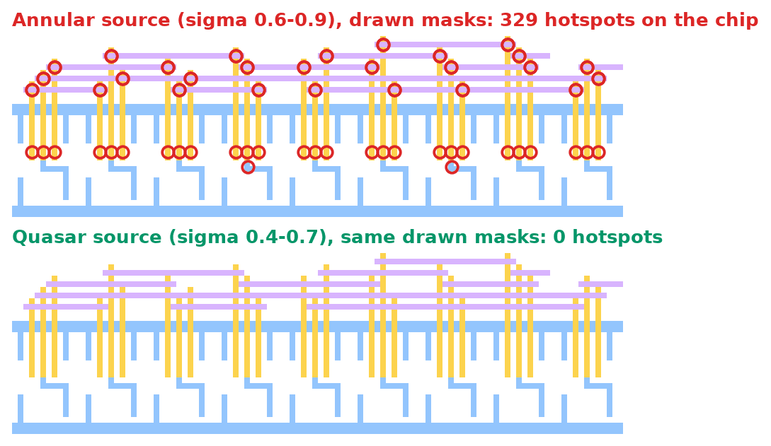
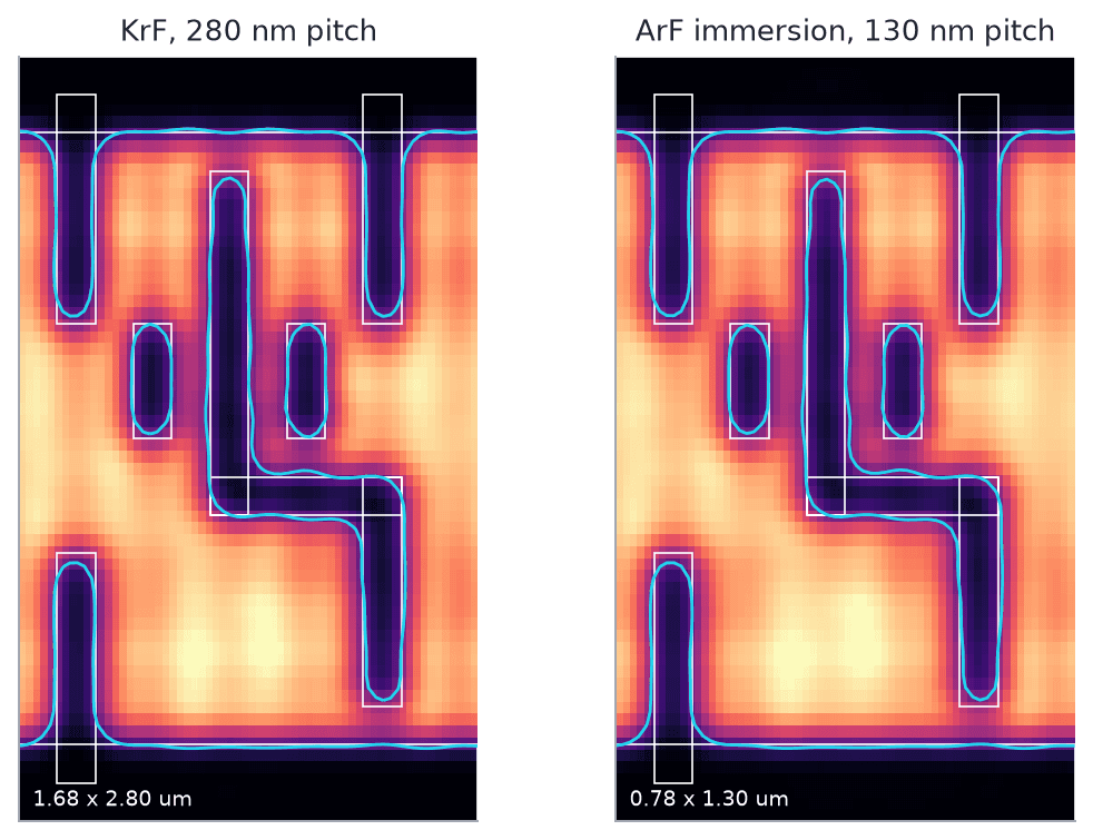
It also shows where a scanner stops. Drawn at a 40 nm metal pitch, the same adder fails on 193i as a single exposure: that is the point where a fab needs EUV or pitch splitting, and the toolkit says so before a mask is made.
Why build this
Commercial tools are tuned to the scanners of the companies that build them. A newer scanner maker, or a research fab running its own process, gets a generic model at best. A toolkit built from the optics up can be fitted to any scanner: its real illumination, its measured lens errors, its process. That matters for anyone building semiconductor capability outside the usual supply chain, and in India most of all.
What’s next
Calibration on real silicon
Fit the models to one real scanner and a test reticle with CD-SEM data. The step that turns a simulator into a production model.
Multipatterning for DUV
Split layouts below the single-exposure limit into LELE, SADP and SAQP masks, then print and check every mask.
Process-window correction
Mask correction that holds across focus and dose, not just at the nominal setting.
Full-chip speed
Whole-layer imaging on the GPU, aiming at hours per square millimetre.
Fitting into real flows
Design-rule checks, OASIS and LEF / DEF, and hotspots in a form a router can avoid.
E-beam direct write
Proximity correction for electron-beam lithography, on the same correction engine.
To be clear about where it stands: these are simulation results. The models are checked against physics and other solvers, not yet against wafers from a real scanner. That is the next step, and the one I’m looking for partners for.
Early access
Running a fab, a scanner, or a process line?
The toolkit is not public. I’m opening it to a small number of fabs, scanner makers and research labs who want to try it on their own machines and layouts, starting with a short demo.
Request access ↗hello@chaii.wtf